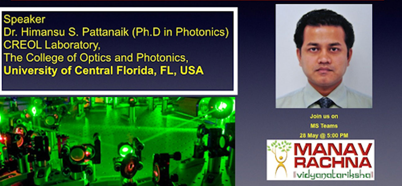
Resource Person:
- Dr. Himanshu S. Pattanaik, CREOL Laboratory, The college of optics & photonics, University of central Florida, FL, USA
Department of Physics, Manav Rachna university organized a research webinar on “Two photon absorption in bulk semiconductors and quantum well structures and its applications” by Dr. Himansu S. Pattanaik from “The College of Optics and Photonics”, University of Central Florida, FL, USA on 28 May 2019 through zoom platform. In his talk, he addressed the possible applications of two-photon absorption (2PA), in direct-gap semiconductors and quantum-well (QW) semiconductor structures. One of the applications is using extremely nondegenerate (END) 2PA, for mid-infrared (mid-IR) detection in uncooled semiconductors. The use of END, where the two photons have very different energies gives strong enhancement compared to degenerate 2PA. This END-2PA enhanced detection is also applied to mid-IR imaging and light detection and ranging (LIDAR) in uncooled direct-gap photodiodes. The 3-D gated imaging system described could be used for examination of buried structures (microchannels, defects etc.) or laser written volumetric structures and could also be suitable for in-vivo imaging applications in biology in the mid-IR spectral region. As an example, 3-D imaging of buried semiconductor structures were presented.


