ICT program on VLSI Design Conducted by ECE, MRU under Aegis NITTTR, Chandigarh
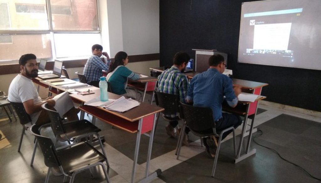
This one-week long program was coordinated by Dr. Y K Awasthi & Ms. Yogita Khanna from MRU, Faridabad. The program proved beneficial for the 12 participants as new technologies were discussed by the resource persons.


The resource persons that endow the program have significant experience in their domain that made the training quiet interactive. The program was embraced by renowned persons from various organizations viz. Dr. Rajesh Mehra from ECE Department, NITTTR, Chandigarh, Er. H. S Jatana from Semiconductor Laboratory, Mohali, Ms. Pooja Dhankar, Semiconductor Laboratory, Mohali, Rajesh Srivastava Semiconductor Laboratory, Mohali, Er. Amit Saini, Cadre Design System , New Delhi, Dr. Rohit Sharma, ECE Department, IIT Ropar, Dr. K G Sharma ECE Department CCET Chandigarh.
The Topics covered during the training of VLSI Design were follows:
(a) CMOS Design & Analog CMOS Design
(b) Advanced MOSFET Devices
(c) Physical Design Implementation & System on chip
(d) Digital Design – Synthesis & APR
(e) High Speed Interconnects
(f) Graphene Nano Ribbons
(g) Fin FET Design
In addition of VLSI Design following issues were discussed:
(i) Design Optimization
(ii) Constraints in Analog Design
(iii) Design Issues & Challenges